Overview
CAD Software
PCBs are designed using KiCAD, which is an open-source tool for PCB design. Design files can be found in the hardware/V1_revB folder of the Github repository:
0_ramn contains design data for RAMN’s main PCB.
1_screens to 5_debuggers contain design data for RAMN’s expansions.

PCB CAD view of RAMN in KiCAD

3D view of RAMN in KiCAD
Design
RAMN’s main board is a credit-card size PCB with 4 ECUs, a CAN FD bus and a USB port.
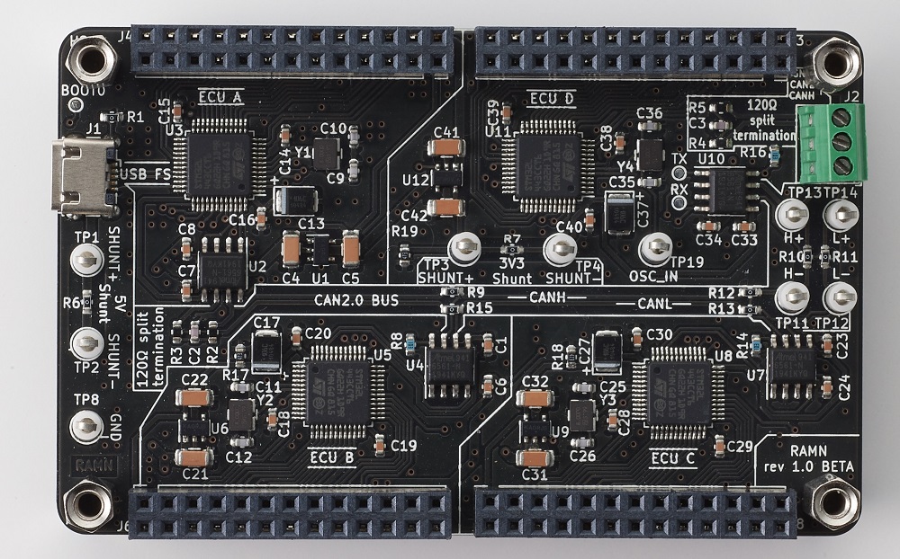
Main board of RAMN
RAMN’s main board can be expanded with expansions boards to add features such as sensors and actuators.
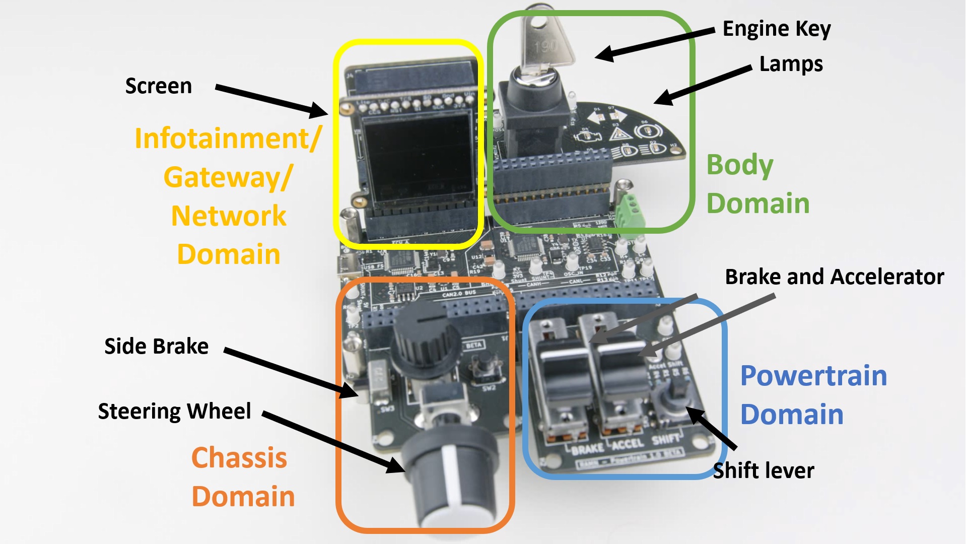
Simple setup of RAMN with 4 expansions: SCREENS (GATEWAY), CHASSIS, POWERTRAIN, BODY.
ECUs (Electronic Control Units)
There are 4 ECUs on RAMN (ECU A, ECU B, ECU C, and ECU D), and they all share a common design:
ECU A additionally features a USB connection. The USB port is the main 5V power supply for the whole board, and is also used as a means to reprogram all ECUs. ECU A has 6 GPIOs that are used to control:
The power supply of ECU B, ECU C, and ECU D
The boot mode (BOOT0 pin) of ECU B, ECU C, and ECU D
ECU D has an additional shunt resistor and clip-on probes for easier measurements.
CAN/CAN FD bus
RAMN features a CAN FD bus that connects the 4 ECUs and is terminated on both sides by 120 ohm split-terminations.
By default, RAMN only uses classic CAN messages and can be used with classic CAN controllers.
The CAN FD bus features shunt resistors and clip-on probes for easier measurements as well.
The CAN FD bus can be accessed from outside through a terminal block.
Block Diagrams
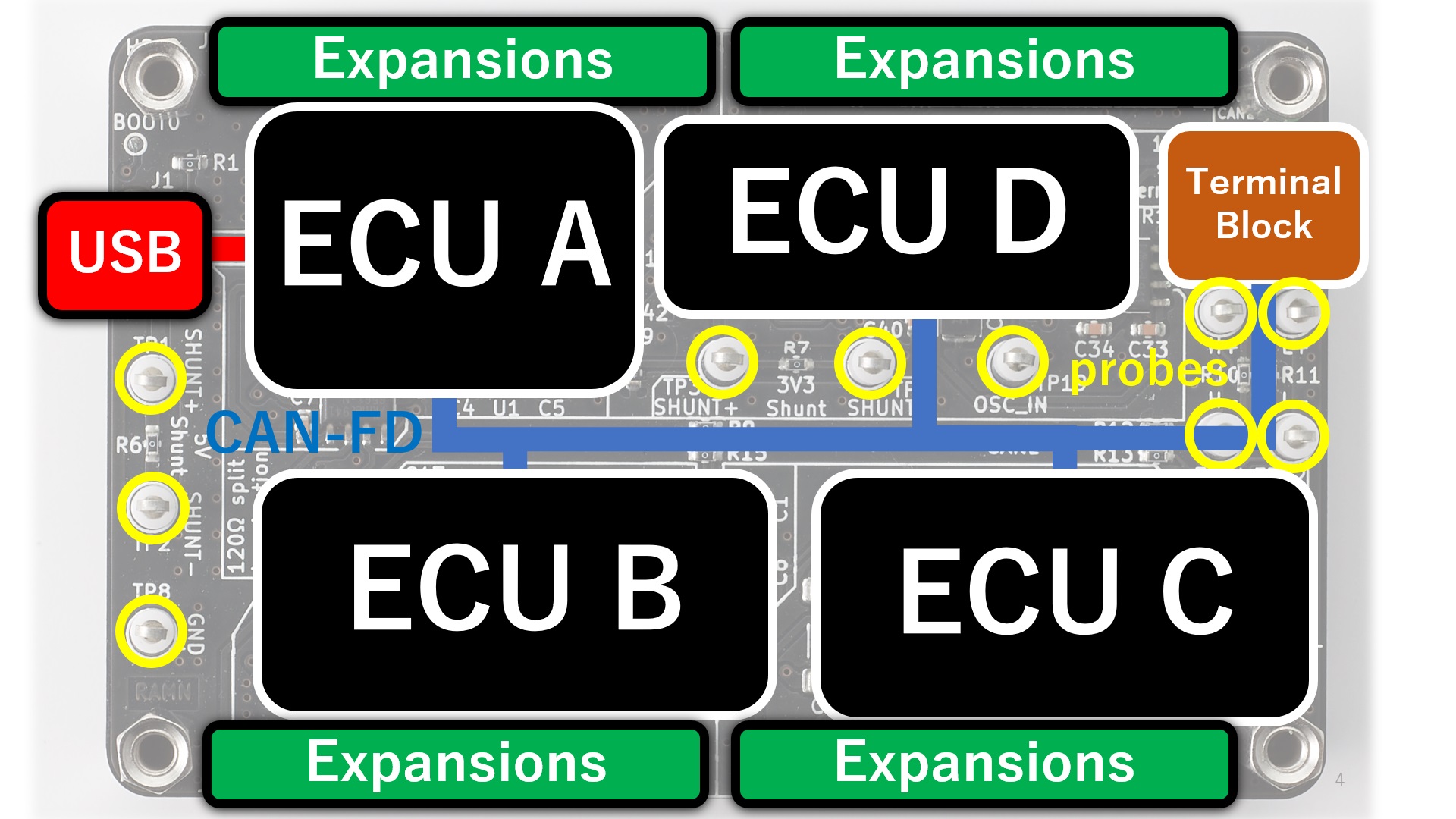
Simple Block diagram of RAMN’s main board.
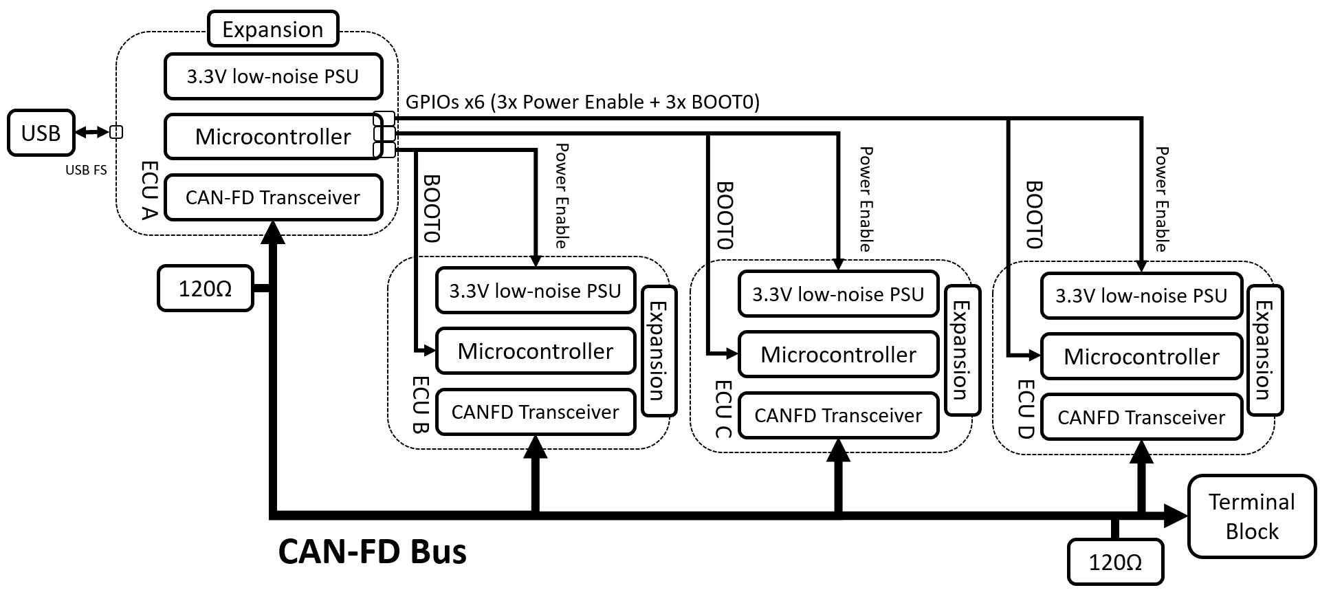
Block Diagram of RAMN showing connection between ECUs.
Hardware Design Rules
Guidelines
RAMN aims to promote education and research in automotive systems. To stay close to automotive electronics, we use AEC-Qxxx grade 0 (or equivalent) components for the ECU network board. To keep the board small and affordable, many protections (e.g. ESD protection, pull-up/pull-down resistors, etc.) are omitted, and the board would not meet reliability levels required in safety-critical systems.

Picture of RAMN PCB’s front side, before components soldering.

Picture of RAMN’s PCB’s back side, before components soldering.
All boards are designed using only two layers, with all components on the same side. The boards have large manufacturing tolerances (e.g. large track width and clearance), and we restrict components to those with visible external pins, unless there really is no viable alternative. All those elements ensure that the PCBs can be manufactured and assembled at a low cost. The board is also accessible to hobbyists who would like to fabricate and solder the board themselves.

Design tolerances for RAMN’s PCB.
Impedance Matching
Since frequencies involved in RAMN are relatively low, proper impedance matching is not a high priority. However, good design guidelines are followed when possible.
CAN/CAN-FD Bus
Although the quality of the CAN/CAN-FD bus line is limited by the tight layout, the many connections, and the use of only 2 layers, we tried to keep a 120 ohm differential impedance on the CAN-FD bus. More precisely, we used a trace width of 0.45mm and a spacing of 0.2mm, which according to EEWeb’s Edge Coupled Microstrip Impedance calculation tool, should lead to a 120 ohm differential impedance on a standard 35um copper 1.6mm FR-4 thick layout.

Layout of the CAN-FD bus.
USB
For the USB line, no impedance matching is attempted. Instead, we follow FTDI’s recommendations for USB hardware design:
Equal length for D+ and D-
Ground plane under the D+ and D-
Etc.

Layout of the USB connection.